
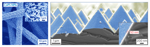
Scientists discovered that a close relative of a well-known iron-based mineral called fool’s gold (iron pyrite, FeS2) is an
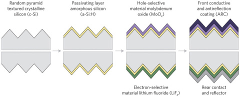
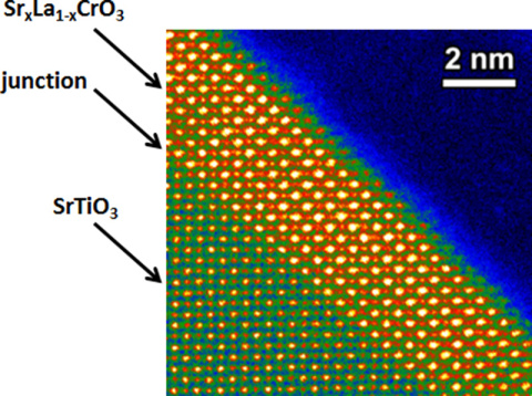
In this simplified architecture, sunlight passes through the top layer (metal oxide) and creates electron-hole pairs in the silicon. The holes are
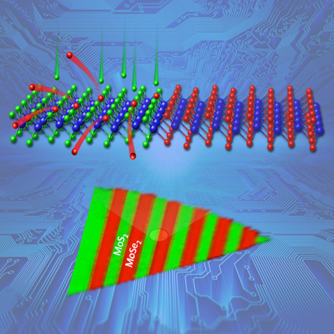
Junctions of two-dimensional (2D) semiconductors could enable next-generation photovoltaics, lighting, and electronics. For example, current
A new ultra-thin semiconducting material (tungsten disulfide or WS2) consists of three atomic layers in an “atomic sandwich”
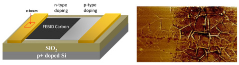
Scientist have developed a novel “direct-write” additive lithographic technique that can be used to electronically pattern graphene
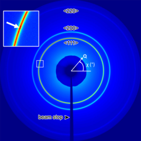
Conventional transmission electron microscopy and metallography techniques survey a limited amount of material in samples. Consequently, these
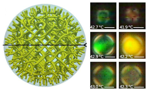
Biology uses stress, defects, molecular configuration (for example, handedness), and hierarchical design strategies to assemble and/or create a
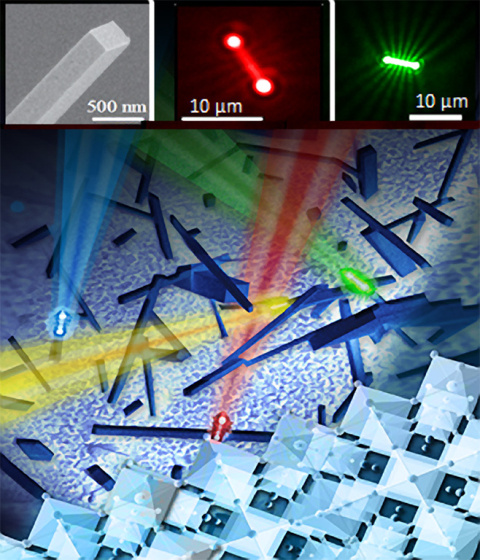
Semiconductor nanowire lasers, due to their ultra-compact physical sizes, highly localized coherent output, and efficiency, are promising
Numerous applications from flat panel displays to solar cells require high-performance transparent conducting oxides. Commercial applications

3D printing has revolutionized the way we can make and design materials. Now a team led by scientists at Oak Ridge National Laboratory has added