
With a twist between layers of graphene, scientists supported by the DOE’s Office of Science created the foundation for twistronics.
September 8, 2026 Estimated Read Time min
Shannon Brescher Shea

Shannon Brescher Shea (shannon.shea@science.doe.gov) is the social media manager and senior writer/editor in the Office of Science’s Office of Communications and Public Affairs. She writes and curates content for the Office of Science’s Twitter and LinkedIn accounts as well as contributes to the Department of Energy’s overall social media accounts. In addition, she writes and edits feature stories covering the Office of Science’s discovery research and manages the Science Public Outreach Community (SPOC). Previously, she was a communications specialist in the Vehicle Technologies Office in the Office of Energy Efficiency and Renewable Energy. She began at the Energy Department in 2008 as a Presidential Management Fellow. In her free time, she enjoys bicycling, gardening, writing, volunteering, and parenting two awesome kids.
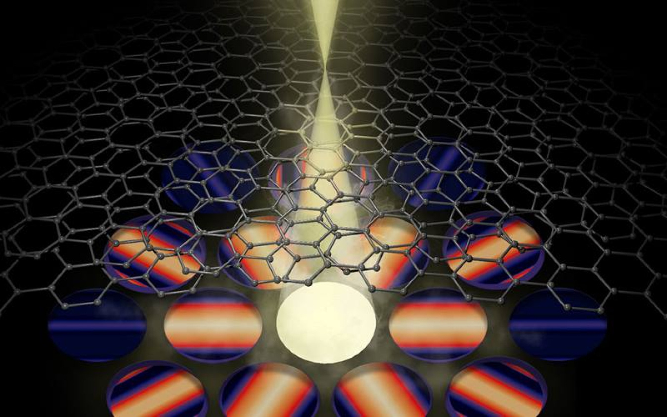
Placing two lattices – like window screens – on top of each other and twisting one layer compared to the other creates intriguing patterns. In fact, there are toys based on the designs that emerge, called moiré patterns.
But moiré patterns aren’t just visually interesting. At the nanoscale, this phenomenon reveals properties that could form a foundation for new technologies.
In 2009, a team led by Eva Andrei at Rutgers University supported by the Department of Energy’s (DOE) Office of Science started researching stacked layers of two-dimensional materials. Two-dimensional materials are only a single atom thick. They have bizarre properties compared to their thicker cousins. For example, graphene is the flat, two-dimensional version of graphite – the “lead” material in pencils. Despite the fact that graphite is soft, graphene is the strongest material ever found. What Andrei’s team found led to a whole new field of research in physics, called “twistronics.”
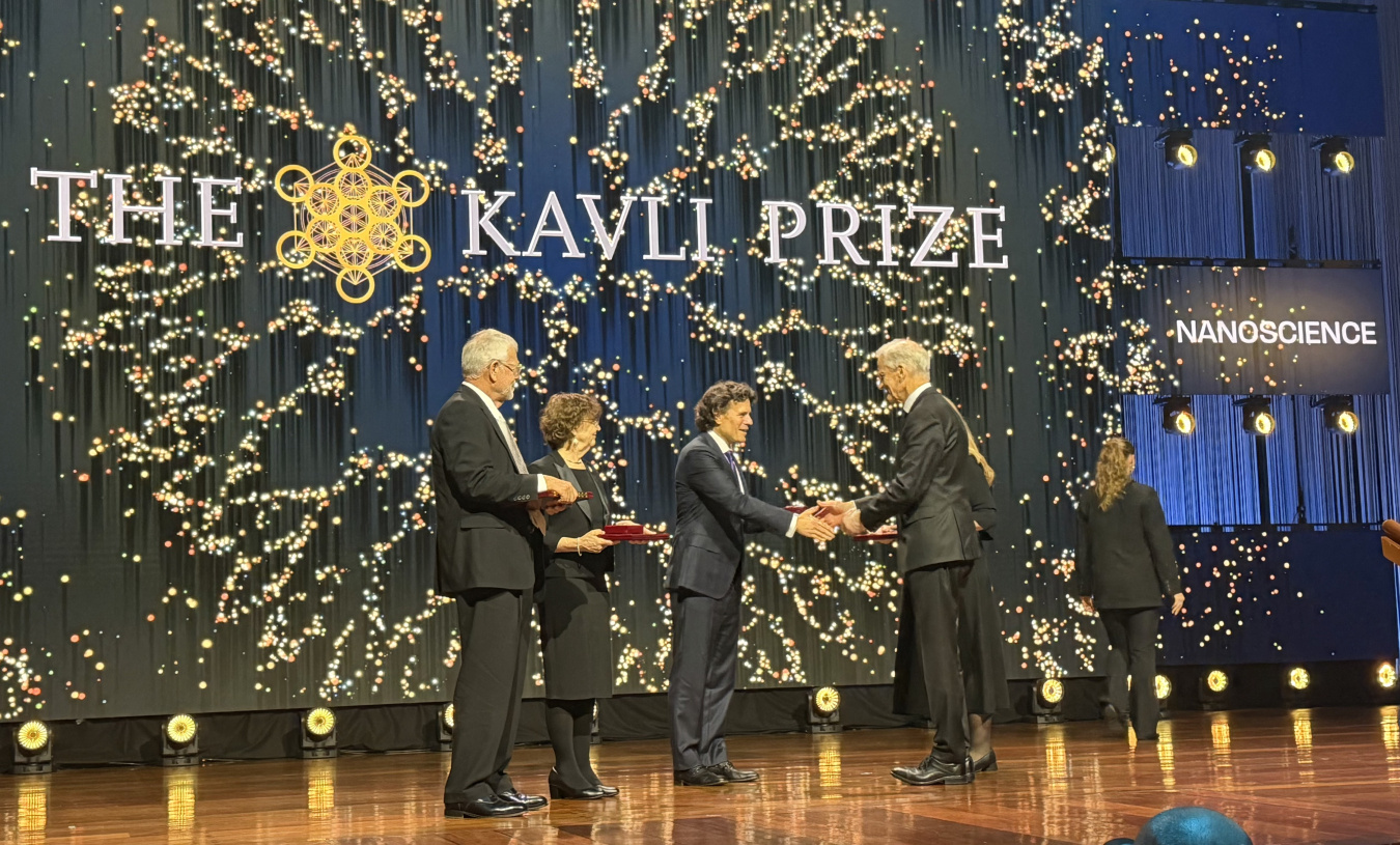
The prestigious Kavli Prize in Nanoscience recently recognized Andrei as well as Pablo Jarillo-Herrero and Allan H. MacDonald for their contributions. DOE’s Under Secretary for Science Darío Gil recently attended the Kavli Prize ceremony to congratulate Andrei and celebrate her award.
Together, these award-winning scientists laid the foundations for work that researchers at DOE’s National Laboratories and other institutions are pursuing today.
The unusual case of graphene
At the time of the 2009 discovery, Andrei was no stranger to 2D materials. Researchers discovered graphene in 2004; her team started working with it not long after. In fact, her undergraduate thesis years earlier dealt with a “cousin” to graphene that became important in twistronics later on.
Andrei and her team were interested in graphene because of the unusual way electrons move within it. The honeycomb pattern of graphene’s carbon atoms makes it amazing at conducting heat and electricity.
In the early days of graphene research, many materials scientists thought electrons didn’t interact very much in graphene, like in most materials. Andrei’s team found evidence otherwise. That discovery netted them an article in Nature magazine and a spot in the Top 10 Scientific Breakthroughs of the Year in Science.
Following how electrons move
Finding signs of these strong interactions led Andrei to investigate other strange features of graphene’s electronic structure. Understanding how electrons move through materials holds the key to unlocking new areas in physics and developing new technologies.
Imagine an individual atom, as you might read about in a high school physics textbook. There is a nucleus with protons and neutrons; electrons swirl around that nucleus. Each electron rotates around the nucleus in a specific, clear energy level. The area it spins in is called its atomic orbital.
When two atoms get near each other, the orbitals of the outermost electrons overlap. The electrons can now move from atom to atom. This movement splits the initial atomic orbitals into new ones – molecular orbitals. Each of these new orbitals is at a different energy level. When thousands of atoms in a solid come together, it creates an astronomical number of orbitals and energy levels.
There are so many of these energy levels that they cram together with no spaces in-between. Materials scientists call these connected states a “band.” These bands are ranges of energy levels that electrons can occupy. There are also some places where there are no orbitals that electrons can occupy. This space is a gap in the bands, or a band gap. For an electron to move from one band (or range of energy levels) to another, it needs enough energy to “jump” the band gap.
The electronic structures that these bands and band gaps form determine if a material is a metal that conducts electricity, an insulator that doesn’t, or a semi-conductor. All three are essential in electronics. You want copper wires that conduct electricity and insulating materials that prevent you from getting electrocuted. Meanwhile, semiconductors are essential to computer chips.
In addition to everyday applications, bands and band gaps are important for quantum material scientists. The density of state, or how many electrons can share the same combination of speed and energy (or space and time), is an important characteristic. At some energy levels, lots of electrons can share the same space and time. In others, no electrons can. When you reach a band gap, the density of states drops to zero.
Big changes in the density of state can indicate changes in how electrons are moving in a material. That’s what Andrei and her group saw in the stacked layers of graphene – although it was completely by accident.
An accidental stacking
When Andrei and her group sought to study graphene as part of the study supported by DOE’s Office of Science, they expected to be examining a single sheet. The original aim was to study a large sample of graphene with a transmission electron microscope.
After a process that involved multiple universities and a trans-Atlantic trip, Andrei’s group received their sample. As it turned out, the person who created it at the Massachusetts Institute of Technology (MIT) used a base made of nickel instead of copper. Coincidentally, that change produced multiple stacked layers of graphene. As Andrei said in her personal reflection for the Kavli Award, “What we saw was a complete surprise—not even close to what we expected.” Moreover, each layer was off from the other just a little bit. The graphene production had accidentally produced moiré patterns.
The existence of moiré patterns in graphene wasn’t new. But what the team did next was – they started investigating the patterns’ electronic properties. They found that the band structure – the bands and band gaps in the material – was very different in the twisted bilayer graphene than in the single sheet. That meant the electronic structure would be different too.
Because the material had layers at different angles from each other, the team could study the effects of these angles on the electronic structure. They discovered one particular twisted angle – 1.07 degrees – that had a strangely “flat” electronic band. In these bands, energy levels are squeezed together. As a result, far more electrons can occupy the same energy level than usual.
That finding changed everything. This radical increase in density of state is associated with electrons moving in a coordinated way. This collective action is in contrast to electrons’ usual disorganized movement. Strongly interacting electrons lead to a number of strange quantum properties. One of these properties is superconductivity, when electricity can run through a material without resistance. Figuring out how to create superconducting materials that work near or at room temperature would expand the possible applications for superconductors.
Next steps in twisting
The potential to control how electrons move in 2D materials with a twist opened the door for all sorts of possibilities.
But first, physicists had to understand why it happens. In 2011, Allan H. MacDonald’s team at the University of Texas at Austin developed a theoretical model of this phenomenon. This analysis helped scientists understand what barriers stood in the way of manipulating these 2D layers.
In 2018, Pablo Jarillo-Herrero and his group at MIT built on Andrei’s discovery. Recreating parts of the initial discovery, they twisted sheets of graphene to the “magic angle” of 1.07 degrees. With more in-depth experimentation, they demonstrated that this angle resulted in unconventional superconductivity. While most materials need to be barely above absolute zero to become superconducting, unconventional superconductors work at slightly higher temperatures. The electrons inside of them also behave differently. These types of materials are the best candidates for potentially creating room temperature superconductors. His team also discovered correlating insulating states, where electrons act in tandem but stop moving.
The potential of twistronics
Since then, the field of “twistronics” has exploded. It offers potential breakthroughs in computing, quantum sciences, and designing custom materials.
Traditionally, scientists have changed materials’ electronic structures and properties by changing their chemistry. Adding or subtracting atoms of different elements can turn an insulator into a conductor or even a superconductor.
In contrast, twistronics allows scientists to control how electrons move through a material by altering its geometry. This finding opens the door to designing smaller and more efficient devices. It could also be an important aspect of more reliable energy storage. Because of moiré superlattices’ quantum properties, they could also be important for quantum computers and other quantum technology.
The future of a field
In the years since 2018, researchers supported by the DOE Office of Science have found ways to manipulate moiré superlattices, unique quantum states of matter, methods to analyze the superlattices, and different ways to make them.
- At Columbia University in 2019, researchers confirmed the 2018 MIT results. They also found that applying pressure to twisted bilayer graphene allows researchers to adjust the layers with more flexibility in terms of reaching the magic angle.
- In 2020, scientists at DOE’s Lawrence Berkeley National Laboratory observed exotic states of matter in a moiré superlattice created from a different 2D material.
- Researchers at Columbia University and California Institute of Technology (CalTech) both started stacking three layers of graphene, finding that it increases the chances of achieving superconductivity. The CalTech researchers also demonstrated that they could use an electric field to manipulate the material.
- At DOE’s Oak Ridge National Laboratory, researchers have developed new ways to take images of stacked 2D materials. They also created an artificial intelligence program to identify the location of atoms and describe their structure.
- This year at Cornell University, researchers developed a simpler process to create moiré superlattices. By pulling and compressing the upper layers instead of twisting them, they created different geometries. As this process is already common in semiconductor manufacturing, it may be easier to scale up.
These are only a few of the advances made in twistronics over the last decade. With more tools available than ever, the opportunities will only expand. An accidental creation combined with curiosity set the foundation for an entirely new field of research.