
With the help of DOE funding, Applied Materials has developed an advanced epitaxial growth system for gallium nitride (GaN) LED devices that decreases operating costs, increases internal quantum efficiency, and improves binning yields.
The standard epitaxy method uses a single metal-organic chemical vapor deposition (MOCVD) chamber for each of the three principal layers of an LED structure, which slows down the production process and requires costly and time-consuming cleaning after each step. Applied Materials' method, however, uses a separate MOCVD chamber for each layer, which facilitates optimization, as well as a self-cleaning process that adds further efficiencies.
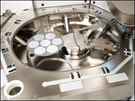
In addition, a faster and cheaper new technology, hybrid vapor phase epitaxy (HVPE), is used instead of MOCVD for one of the steps. HVPE technology has been around for 50 years and at one time was widely used for growing GaN, but the industry switched to MOCVD because of better reproducibility. Applied Materials has solved that problem with a unique HVPE chamber architecture that enables repeatability and features the largest reported chamber size in the industry. The project involves the first large-scale HVPE tool capable of high-volume LED production, and the results show excellent run-to-run wavelength uniformity over 100 runs.
Return to Research Highlights