
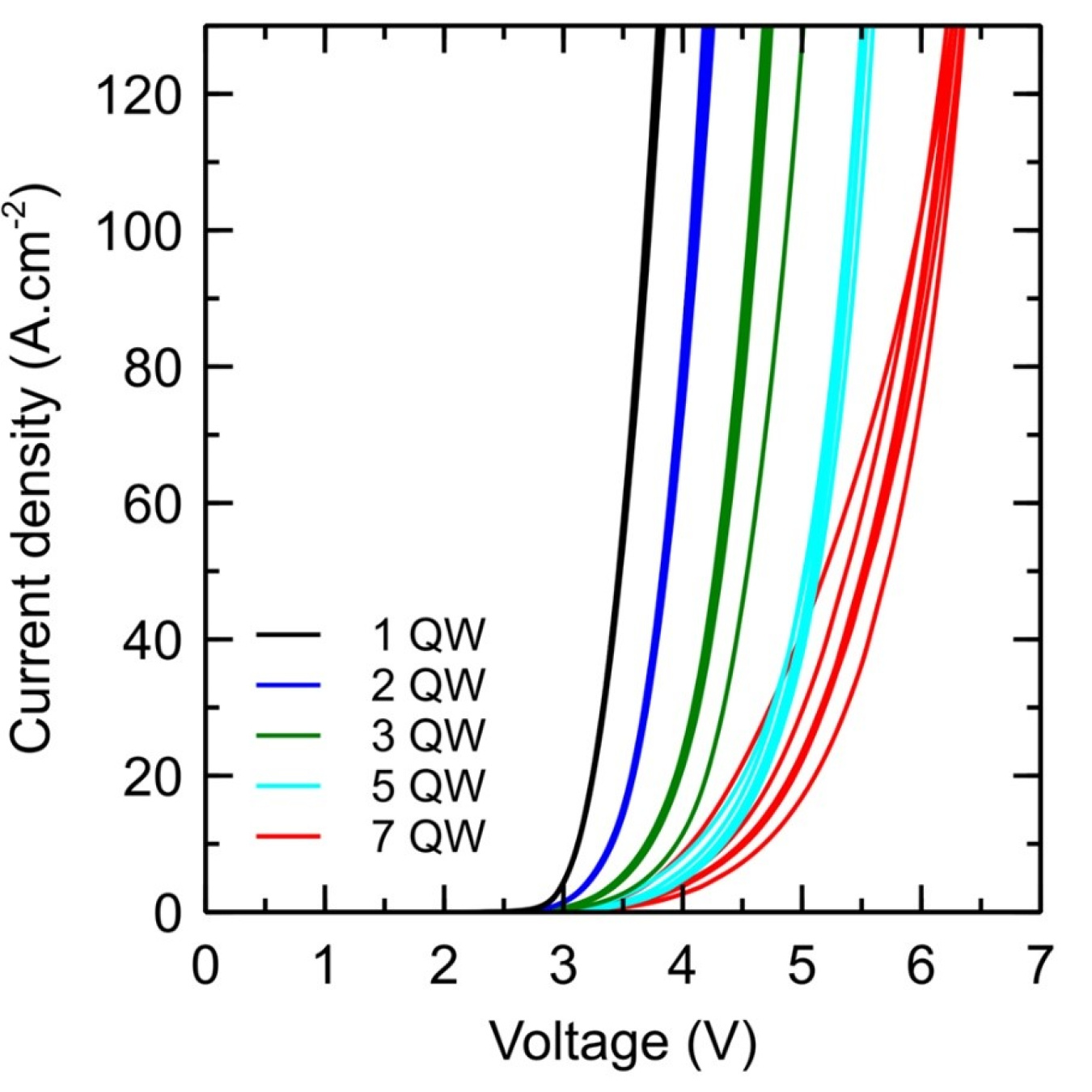
Current density vs. forward voltage for green LEDs with increasing number of quantum wells (QWs). More QWs resulted in higher forward voltage.
Light-emitting diodes (LEDs) based on Group III nitrides (III-N) are attractive for general illumination because of they can emit light in nearly the entire visible spectrum. Recent R&D efforts in LED lighting have focused on increasing the efficiency of green emitters, with the additional goal of improving the efficiency of III-N-based yellow and amber LEDs. The development of efficient longer-wavelength III-N emitters remains a major opportunity for higher energy savings by enabling a color-mixed LED approach, which uses a mixture of red, green, and blue LEDs to produce white light with higher efficiency than conventional phosphor-converted LEDs. However, today’s green LEDs suffer from larger excess forward voltage (ΔVF) and lower quantum efficiency relative to their blue counterparts.
Using a computational approach based on landscape theory, researchers at the University of California at Santa Barbara (UCSB) have identified key factors in the LED’s semiconductor layer structure that impact the forward-voltage performance of green LEDs. The findings indicate that careful design of the semiconductor layers in or surrounding the LED active region is essential to avoid excess voltage in green LEDs. The number of quantum wells (QWs), the percentage of aluminum in the quantum barriers, and the InGaN/GaN superlattice structure below the LED active region can be optimized to reduce the forward-voltage penalty in green LEDs.
The researchers found that unlike blue LEDs, which do not incur a VF penalty with an increased number of QWs, the number of QWs significantly increases VF in green LEDs – which is in close agreement with the researchers’ 3D simulation results. This supports previous findings that strain effects at the interfaces in the active region from lattice mismatch between InGaN QWs and GaN barriers slow efficient carrier transport into the QWs. The 3D simulations show that sequential injection of the QWs also contributes to the high VF in these structures.
The UCSB team further reduced the forward voltage of green LEDs by reducing the Al content of the AlGaN capping layer in the quantum barriers separating QWs, by reducing the GaN quantum barrier thickness, by increasing the number of periods of the InGaN/GaN superlattice layers below the active region, and by improving the p-contact resistance. Still another approach that resulted in reduced voltage was the use of InGaN, rather than GaN, quantum barriers. An area of significant interest for future research involves 3D volumetric injection of carriers into multiple QWs instead of sequential injection into the active region, which is promising for further voltage reduction and reduced droop in long-wavelength LEDs. (September 2019)
Return to Research Highlights.