
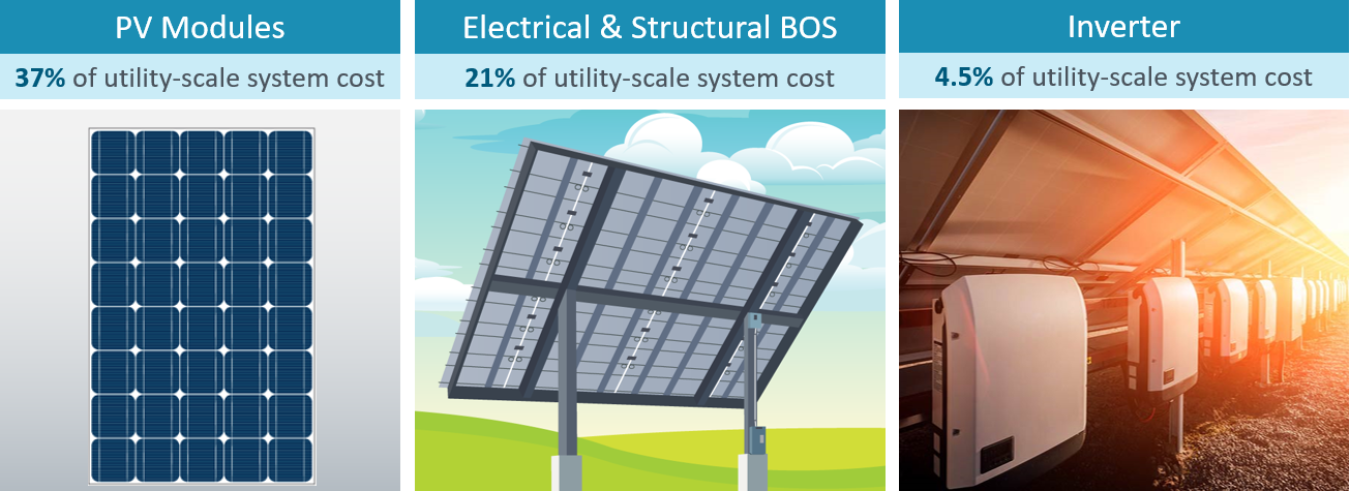
Solar manufacturing encompasses the production of products and materials across the solar value chain. While some concentrating solar-thermal manufacturing exists, most solar manufacturing in the United States is related to photovoltaic (PV) systems. Those systems are comprised of PV modules, racking and wiring, power electronics, and system monitoring devices, all of which are manufactured. Learn how PV works.
Read the Solar Photovoltaics Supply Chain Review, which explores the global solar PV supply chain and opportunities for developing U.S. manufacturing capacity.
PV Module Manufacturing
Silicon PV
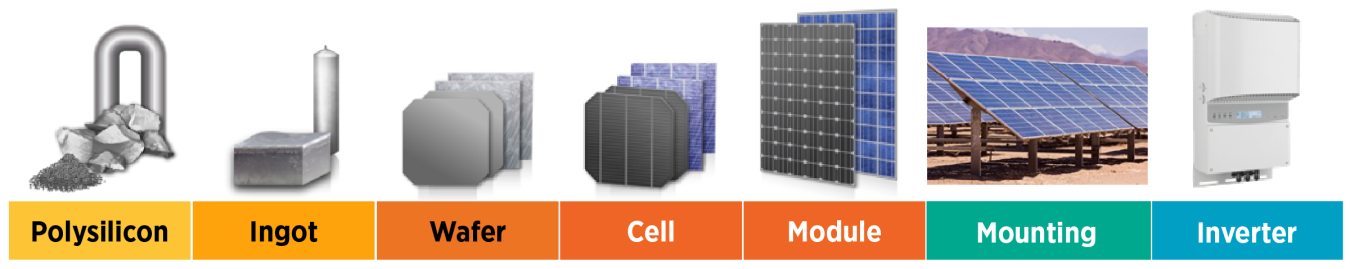
Most commercially available PV modules rely on crystalline silicon as the absorber material. These modules have several manufacturing steps that typically occur separately from each other.
- Polysilicon Production – Polysilicon is a high-purity, fine-grained crystalline silicon product, typically in the shape of rods or beads depending on the method of production. Polysilicon is commonly manufactured using methods that rely on highly reactive gases, synthesized primarily using metallurgical-grade silicon (obtained from quartz sand), hydrogen, and chlorine. In one process, called the Siemens process, the silicon-hydrogen-chlorine compound gas passes over a heated silicon filament, breaking the molecular bonds and depositing the silicon atom on the filament, which ultimately grows into a large U-shaped polysilicon rod. The hydrogen and chlorine atoms are reused in a closed cycle. To keep the filament from contaminating the high-purity poly, the filament itself is also made of pure silicon. In another method, small silicon beads sit at the bottom of an inverted cone-shaped vessel where a compound gas of silicon and hydrogen is pumped in, causing the small beads to float near the surface. Heating the vessel causes the silicon-hydrogen bonds to break, which results in the silicon atoms depositing onto the small beads until they are too heavy to float and drop to the bottom of the vessel where they are harvested, ready for use.
- Ingot and Wafer Production – To turn polysilicon into wafers, polysilicon is placed into a container that is heated until the polysilicon forms a liquid mass. In one process, called the Czochralski process, a large cylindrical ingot of monocrystalline silicon is grown by touching a small crystalline seed to the surface of the liquid and slowly pulling it upward. In another process, call directional solidification, the liquid mass is slowly cooled until it solidifies from the bottom up, forming a large-grained multicrystalline-silicon ingot. Silicon ingots are then sliced into very thin wafers using diamond-coated wire saws. The silicon sawdust that is created is called kerf. Though less common, kerfless wafer production can be accomplished by pulling cooled layers off a molten bath of silicon, or by using gaseous silicon compounds to deposit a thin layer of silicon atoms onto a crystalline template in the shape of a wafer.
- Cell Fabrication – Silicon wafers are then fabricated into photovoltaic cells. The first step is chemical texturing of the wafer surface, which removes saw damage and increases how much light gets into the wafer when it is exposed to sunlight. The subsequent processes vary significantly depending on device architecture. Most cell types require the wafer to be exposed to a gas containing an electrically active dopant, and coating the surfaces of the wafer with layers that improve the performance of the cell. Screen printing of silver metallization for electrical contacts is also very common among cell types.
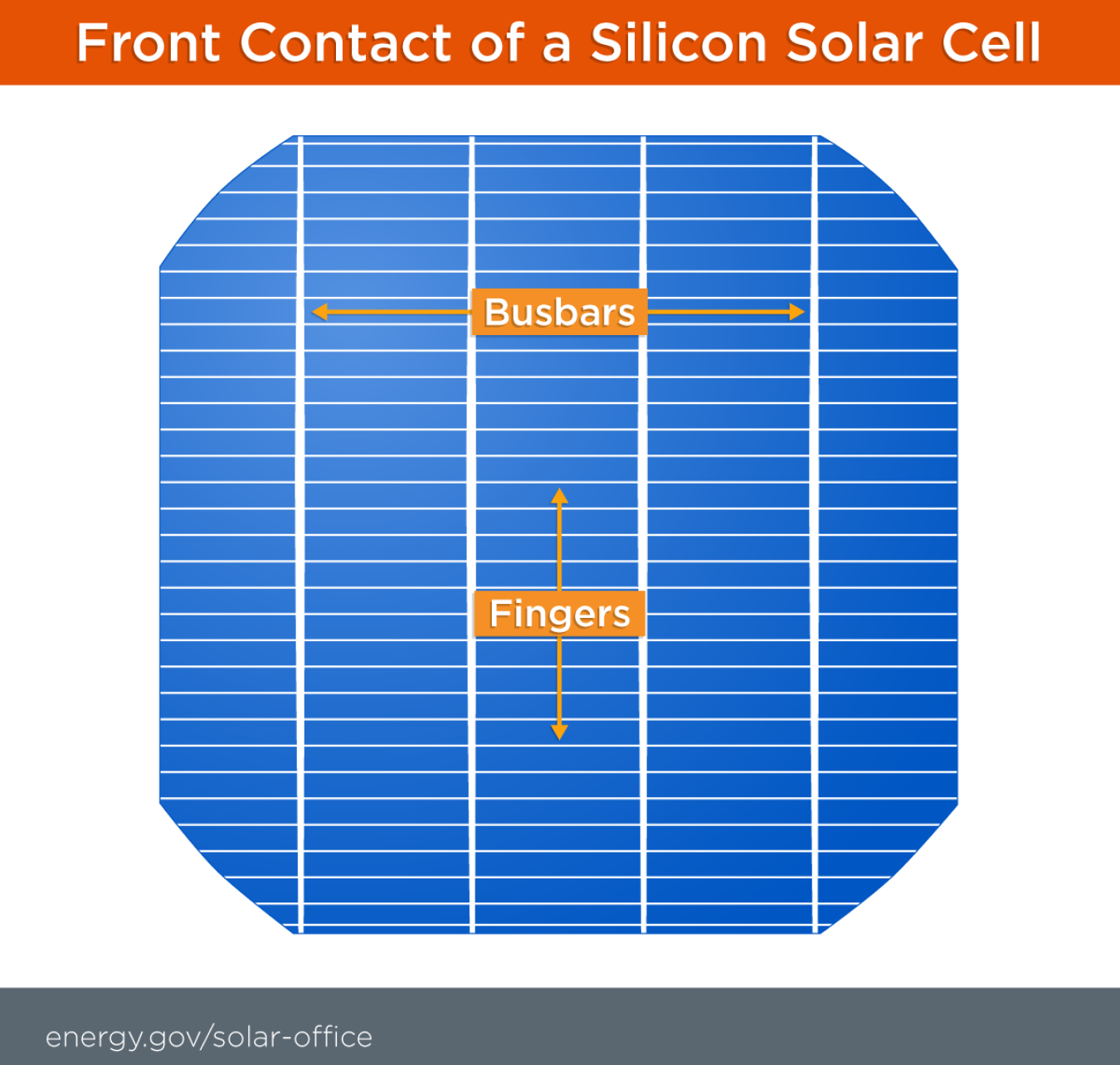
- Module Assembly – At a module assembly facility, copper ribbons plated with solder connect the silver busbars on the front surface of one cell to the rear surface of an adjacent cell in a process known as tabbing and stringing. The interconnected set of cells is arranged face-down on a sheet of glass covered with a sheet of polymer encapsulant. A second sheet of encapsulant is placed on top of the face-down cells, followed by a tough polymer backsheet or another piece of glass. The whole stack of materials is laminated in an oven to make the module waterproof, then fitted with an aluminum frame, edge sealant, and a junction box in which the ribbons are connected to diodes that prevent any backward flow of electricity. Electrical cables from the junction box convey the current produced by the module to an adjacent module or to the system’s power electronics.
Thin Film PV
Thin film PV can refer to a number of different absorber materials, the most common of which is cadmium telluride (CdTe). Thin film PV modules are typically processed as a single unit from beginning to end, where all steps occur in one facility. The manufacturing typically starts with float glass coated with a transparent conductive layer, onto which the photovoltaic absorber material is deposited in a process called close-spaced sublimation. Laser scribing is used to pattern cell strips and to form an interconnect pathway between adjacent cells. Copper ribbons are applied, an encapsulant sheet and second sheet of glass are placed on top, and the stack is laminated to make it waterproof. Finally, a junction box is attached to the rear of the module. There, the module’s electrical cables are attached to the copper ribbons, which pass into the junction box through holes in the rear glass.
Racking Systems
The support structures that are built to support PV modules on a roof or in a field are commonly referred to as racking systems. The manufacture of PV racking systems varies significantly depending on where the installation will occur. Ground-mounted racking is made from steel, which is typically coated or galvanized to protect from corrosion and requires concrete foundations. Large ground-mounted systems typically use a one-axis tracking mechanism, which helps solar panels follow the sun as it moves from east to west. Tracking requires mechanical parts like motors and bearings. Stationary racking (referred to as “fixed tilt”) can be used as well. Roof-mounted racking depends on the type of roof. For flat roofs, like those on large commercial or industrial buildings, fixed-tilt steel racking is used. It is commonly attached to heavy blocks that sit on the roof. For pitched residential roofs, racking is designed to attach securely to the rafters and hold the modules a few inches above the roof. This allows airflow to cool the rear of the modules, improving their performance.
Power Electronics
Power electronics for PV modules, including power optimizers and inverters, are assembled on electronic circuit boards. This hardware converts direct current (DC) electricity, which is what a solar panel generates, to alternating current (AC) electricity, which the electrical grid uses. Learn more about how inverters work.
Assembly starts with a circuit board template. A solder-paste is printed where small components, like transistors and diodes, are placed using robotics. Sometimes, larger components such as capacitors and transformers are placed by hand on the board. Once all components are in place, the board passes across a solder bath in a furnace to connect the components. The entire board is coated with lacquer and sealed into a waterproof housing with ports for external connections.
Learn more about how solar works, SETO's research areas, and solar energy resources.