
DOE invests in multijunction III-V solar cell research to drive down the costs of the materials, manufacturing, tracking techniques, and concentration methods used with this technology. Below is a list of the projects, summary of the benefits, and discussion on the production and manufacturing of this solar technology.
Background
High-efficiency multijunction devices use multiple bandgaps, or junctions, that are tuned to absorb a specific region of the solar spectrum to create solar cells having record efficiencies over 45%. The maximum theoretical efficiency that a single-bandgap solar cell can achieve with non-concentrated sunlight is about 33.5%, primarily because of the broad distribution of solar emitted photons. This limiting efficiency, known as the Shockley-Queisser limit, arises from the fact that the open-circuit voltage (Voc) of a solar cell is limited by the bandgap of the absorbing material and that photons with energies below the bandgap are not absorbed. Photons that have energies greater than the bandgap are absorbed, but the energy greater than the bandgap is lost as heat.
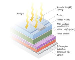
Multijunction devices use a high-bandgap top cell to absorb high-energy photons while allowing the lower-energy photons to pass through. A material with a slightly lower bandgap is then placed below the high-bandgap junction to absorb photons with slightly less energy (longer wavelengths). Typical multijunction cells use two or more absorbing junctions, and the theoretical maximum efficiency increases with the number of junctions. Early research into multijunction devices leveraged the properties of semiconductors comprised from elements in the III and V columns of the Periodic table, such as gallium indium phosphate (GaInP), gallium indium arsenide (GaInAs), and gallium arsenide (GaAs). Three-junction devices using III-V semiconductors have reached efficiencies of greater than 45% using concentrated sunlight. This architecture can also be transferred to other solar cell technologies, and multijunction cells made from CIGS, CdSe, silicon, organic molecules, and other materials are being investigated.
In the past, multijunction devices have primarily been used in space, where there is a premium placed on lightweight power generation, which allows for the use of this relatively high-cost solar technology. For terrestrial applications, the high costs of these semiconductor substrates (compared to silicon, for example) may be offset by using concentrating optics, with current systems primarily using Fresnel lenses. The concentrating optics increase the amount of light incident on the solar cell, thus leading to more power production. Using concentrating optics requires the use of dual-axis sun-tracking, which must be factored into the cost of the system.
Research Directions
Although multijunction III-V cells have higher efficiencies than competing technologies, such solar cells are considerably more costly because of current fabrication techniques and materials. Therefore, active research efforts are directed at lowering the cost of electricity generated by these solar cells through approaches such as developing new substrate materials, absorber materials, and fabrication techniques; increasing efficiency; and extending the multijunction concept to other PV technologies. Furthermore, because of the cost of such solar cells, developing reliable low-cost solutions to tracking and concentration are also active areas of research to support cost reductions for PV systems using multijunction cells.
Learn more about the awardees and the projects involving high-efficiency III-V cells below.
- Ohio State University: Columbus Campus (Photovoltaics Research and Development)
- Arizona State University (Photovoltaics Research and Development)
- University of Oregon (Photovoltaics Research and Development: Small Innovative Projects in Solar)
- South Dakota School of Mines and Technology (Photovoltaics Research and Development: Small Innovative Projects in Solar)
- Arizona State University (Photovoltaics Research and Development: Small Innovative Projects in Solar)
- nLiten Energy (Photovoltaics Research and Development: Small Innovative Projects in Solar)
- University of California, Berkeley (Next Generation Photovoltaics II Projects)
- California Institute of Technology (Next Generation Photovoltaics II Projects)
- North Carolina State University (Foundational Program to Advance Cell Efficiency)
- National Renewable Energy Laboratory (Foundational Program to Advance Cell Efficiency)
- Ohio State University (Foundational Program to Advance Cell Efficiency)
- University of Houston (Next Generation Photovoltaics 3 Projects)
- National Renewable Energy Laboratory (Next Generation Photovoltaics 3 Projects)
Benefits
The benefits of multijunction III-V solar cells include:
- Spectrum matching: High-efficiency cells (>45%) can be fabricated by matching sections of the solar spectrum with specific absorber layers having specific bandgaps.
- Crystal structure: The various combinations of III-V semiconductors have similar crystal structures and ideal properties for solar cells, including long exciton diffusion lengths, carrier mobility, and compatible absorption spectra.
Production
Traditional multijunction III-V cells are assembled in an epitaxial monolithic stack with subcells connected in series through by tunnel junctions. Constructing a multijunction cell in a monolithic stack results in material constraints, and fabricating such devices is facilitated if the individual layers of the subcells have compatible atomic lattice positions and are lattice matched. This advantage of lattice matching is why Ge, which is lattice matched to some III-V alloys, is traditionally used as the substrate and narrow bandgap cell in MJ’s. Lattice matching limitations can be overcome with additional complexity using wafer bonding or metamorphic buffer layers.
The tunnel-junction layer is constructed by the interface of highly doped p++ and n++ layers. The interaction of these layers results in a spatially narrow space-charge region, which allows current to flow between the subcells. High-bandgap layers, known as window layers and back-surface fields, can be added to passivate surface states at the interface between a subcell and the tunnel junction, which if left unpassivated, can trap carriers and accelerate recombination.
If the subcells are connected in series, the subcell that conducts the smallest current limits the maximum current that can flow through the device. Therefore, a considerable effort is placed on tuning the current of the subcells. Luminescent coupling between subcells can relax some of the current-matching design requirements.
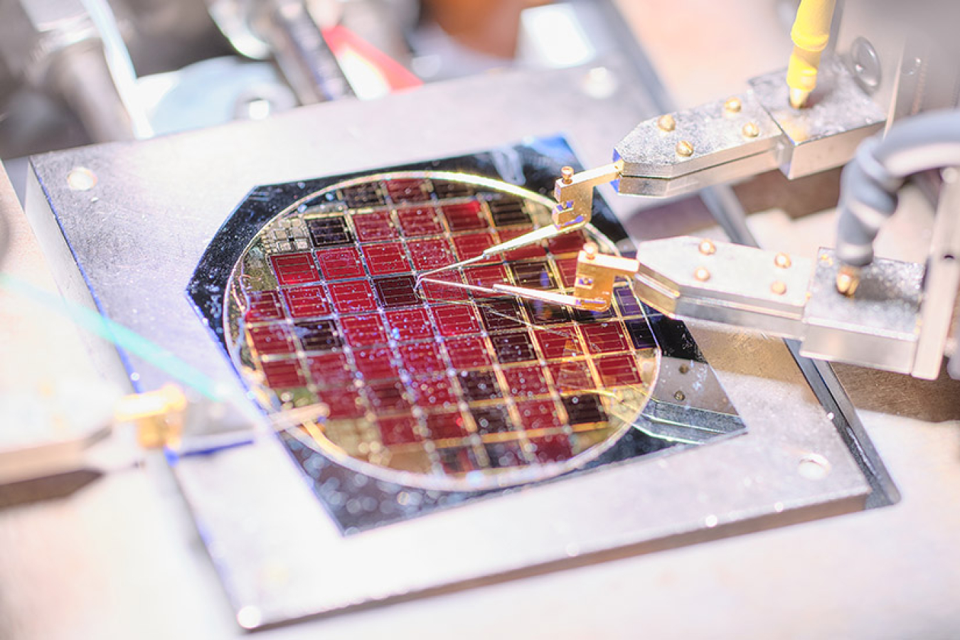
Multijunction III-V solar cells can be fabricated using molecular-beam epitaxy (MBE) techniques, but fabrication in large metal-organic chemical-vapor deposition (MOCVD) reactors is typical for commercial-scale production of GaInP/GaInAs/Ge devices. Layers can be grown from trimethylgallium (Ga(CH3)3), trimethylindium (InC3H9), arsine (AsH3), and phosphine (PH3) in a hydrogen carrier gas and using dopants such as hydrogen selenide (H2Se), silane (SiH6), and diethyl zinc ((C2H5)2Zn). Using concentrating optics allows individual cells to be quite small—at times, as small as the size of the tip of a pencil. Therefore, these techniques allow hundreds of solar cells to be grown in single batches. Research is being done to further reduce the size of cells and increase the number of cells that can be grown from a single wafer, which will help reduce the cost per cell.
For more information on multijunction cells, visit the Energy Basics website.