
Flexible OLEDs are attractive for applications such as displays (produced by Samsung and LG) and solid-state lighting panels (produced by, for example, LG and Konica Minolta), as well as wearable printed sensors. This project investigates the use of corrugated and planarized plastic substrates to increase light extraction from OLEDs; the approach includes development of a buried metal mesh to improve anode conductivity. The fraction of light emitted in the forward direction from conventional, bottom-emitting OLEDs (i.e., the outcoupling factor ηout) is only ~20–25%. This result is due to ~50% loss to internal waveguiding in the high-refractive index [organic+ITO transparent anode] plus excitation of surface plasmons at the flat metal cathode. Another ~25% of the light is waveguided through the substrate to its edges. While extracting the substrate mode with a microlens array or a hemisphere is standard practice, recovering the internally waveguided light and mitigating plasmon losses inexpensively remain challenging. To broadly assess the best designs for enhanced light outcoupling, patterned OLEDs with different corrugation heights and periods—including OLEDs on planarized patterns—were fabricated. To minimize trial and error, substrate designs were guided by simulations, which predict the optimal single- and multi-period structures and the maximum achievable ηout.
The project’s overall goal is to approach ηout = 70% in OLEDs using innovative corrugated as well as planarized patterned light-extraction substrates fabricated in a simple, scalable, and low-cost method that is fully compatible with roll-to-roll (R2R) production. The corrugation results in light diffraction and scattering that minimize internal waveguiding by reducing the total internal reflection at the [organics+ITO]/substrate interface and plasmon loss at the cathode. The project advances the science and technology of OLEDs on plastic substrates, which can be extended to glass substrates as well.
In FY21, researchers continued to fabricate convex and concave patterns on polycarbonate, polyethylene terephthalate (PET), and poly methyl methacrylate (PMMA). The features were of various pitches a (period) and heights/depths h. The pitch a varied from ~400 nm to ~8 mm; h varied from ~50 to ~500 nm. The team achieved external quantum efficiencies (EQEs) of up to 50% for green OLEDs on optimized patterns (in agreement with simulations). Depending on a & h, the OLED stack was either conformal (for a > 2 mm) or partially planarized for narrow pitch values, in particular when associated with tall features.
Because planar OLED substrates are now strongly preferred by panel manufacturers, the project emphasizes "buried" corrugated structures formed in low-index plastic that are planarized ("buried") by a high-index, solvent-free polymer-ceramic composite overcoat layer. Such structures extract otherwise internally lost photons, which are then outcoupled from the substrate to air using an index-matching fluid (IMF) at the substrate/photodetector interface. As shown in the images, EQEs of ~60% have been achieved, approaching the project milestone, using a cost-effective method for two very different buried designs with large heights h > 1.5 mm.
Generating such buried/planarized structures will enable a cost-effective manufacturing approach, as it requires only direct-pattern imprinting into plastic, thereby eliminating time-consuming and expensive steps. Further optimizing the planarized buried designs (including holes/bumps of different diameters as well as dual-pattern formation) should enable low-cost R2R fabrication of light-extracting substrates. (August 2021)
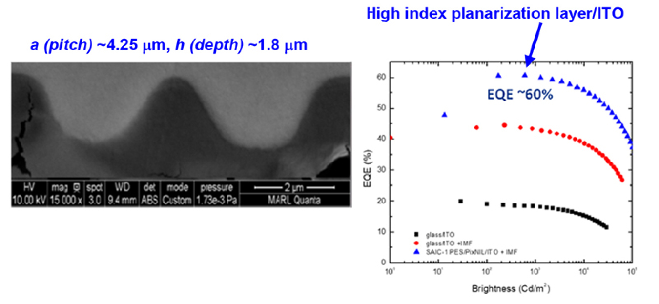
At left, SEM edge images of buried patterns generated by inexpensive direct imprinting in PMMA, planarized by a ~3-4 µm thick high index layer; at right, EQE vs brightness of the enhanced device (blue, maximal EQE ~60%) and glass/IOT reference.