
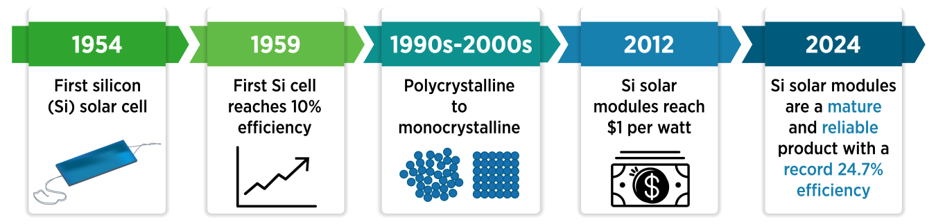
The U.S. Department of Energy (DOE) Solar Energy Technologies Office (SETO) supports crystalline silicon photovoltaic (PV) research and development efforts that lead to market-ready technologies. Below is a summary of how a silicon solar module is made, recent advances in cell design, and the associated benefits. Learn how solar PV works.
What is a Crystalline Silicon Solar Module?
A solar module—what you have probably heard of as a solar panel—is made up of several small solar cells wired together inside a protective casing. This simplified diagram shows the type of silicon cell that is most commonly manufactured.
In a silicon solar cell, a layer of silicon absorbs light, which excites charged particles called electrons. When the electrons move, they create an electric current. In a solar cell, the silicon absorber is attached to other materials, which allows electric current to flow through the absorber layer into the metal contacts and be collected as renewable electricity. Learn more about how solar cells work.
Monocrystalline silicon represented 96% of global solar shipments in 2022, making it the most common absorber material in today’s solar modules. The remaining 4% consists of other materials, mostly cadmium telluride. Monocrystalline silicon PV cells can have energy conversion efficiencies higher than 27% in ideal laboratory conditions. However, industrially-produced solar modules currently achieve real-world efficiencies ranging from 20%–22%.
How are Crystalline Silicon Solar Modules Made?
The manufacturing process for crystalline silicon solar module can be split into 4 main steps (read more about the silicon supply chain):

Material Extraction
Mined quartz is purified from silicon dioxide into solar-grade silicon. There are many smaller steps to this process, including heating up the quartz in an electric arc furnace.
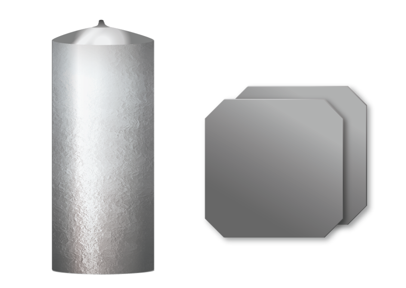
Material Processing
Solar-grade silicon is crushed into chunks and melted. Cylindrical monocrystalline silicon ingots are pulled out of a vat of molten silicon. After cooling, diamond-wire saws are used to slice the ingots into thin wafers.
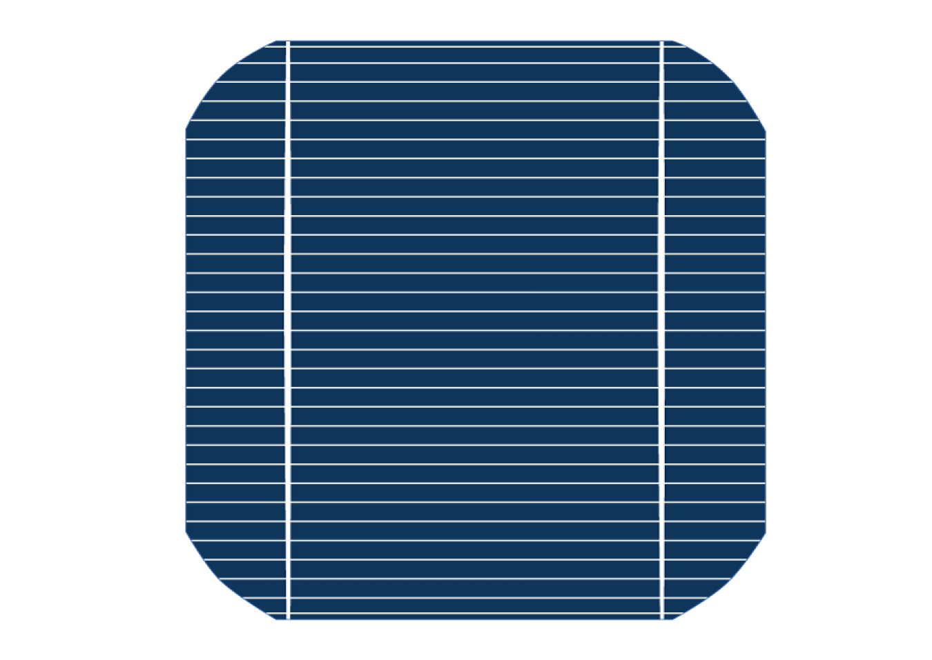
Cell Production
These thin wafers are then processed into solar cells. The exact process for making the solar cell from the wafer depends on the design of the final solar cell. Anti-reflection coatings are deposited on the front surface and electrical contacts are added so electricity can flow.
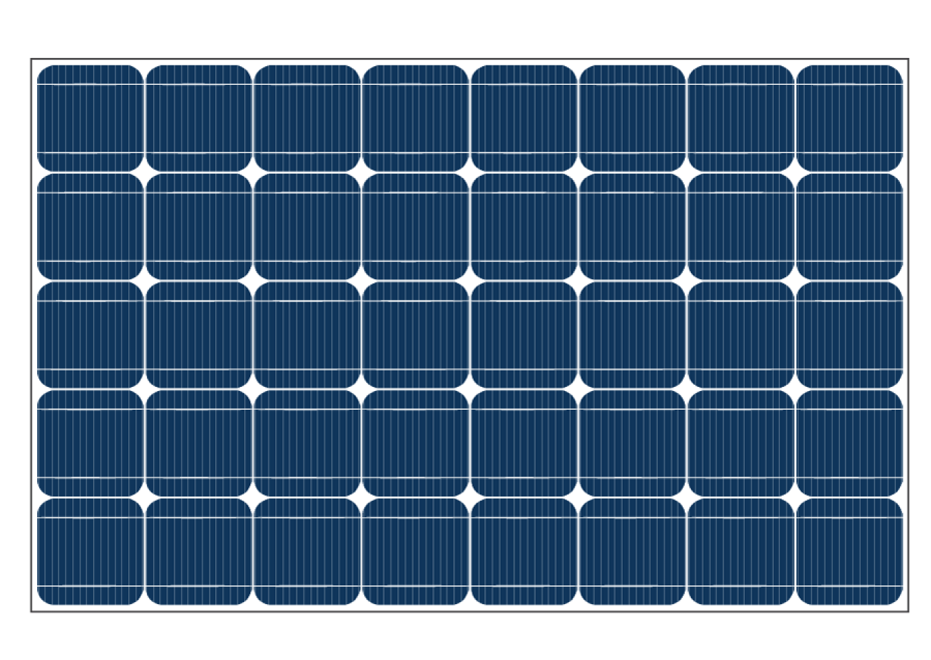
Module Completion
Cells are electrically connected and layered onto glass and plastic sheets for mechanical stability and protection from outdoor conditions. Aluminum framing is typically used around the edges of the module for further reinforcement.

Deployment
The module is ready to be placed on your roof or ground-mounted to generate clean electricity!
What are the Different Types of Crystalline Silicon Solar Cells?
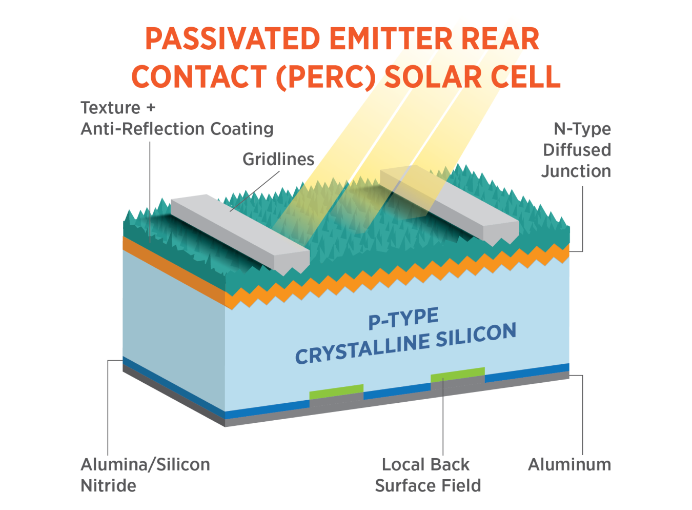
There are several crystalline silicon solar cell types. Aluminum back surface field (Al-BSF) cells dominated the global market until approximately 2018 when passivated emitter rear contact (PERC) designs overtook them due to superior efficiency.
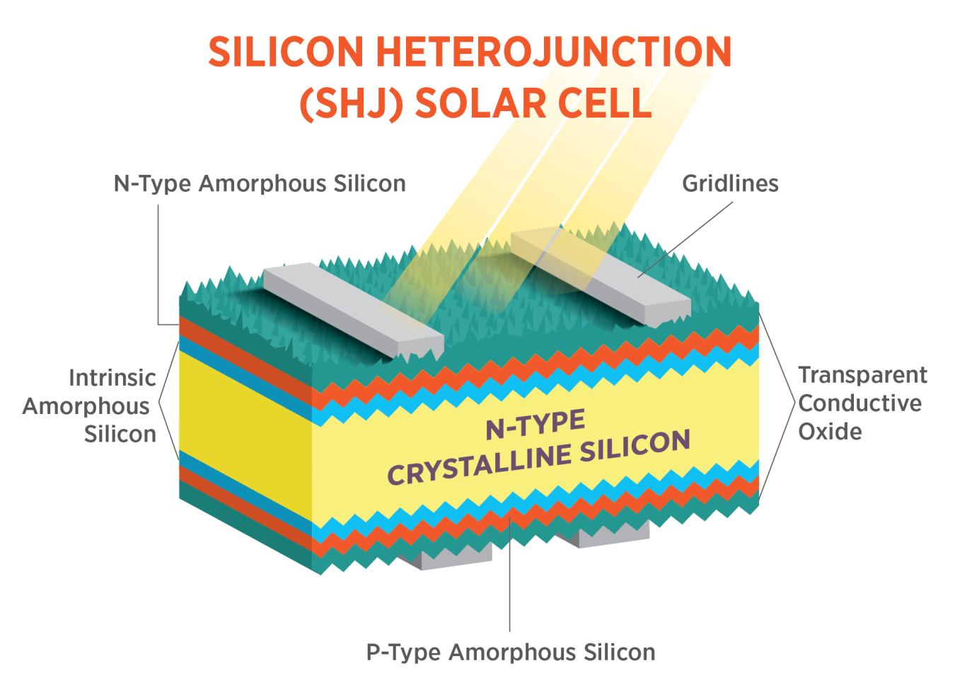
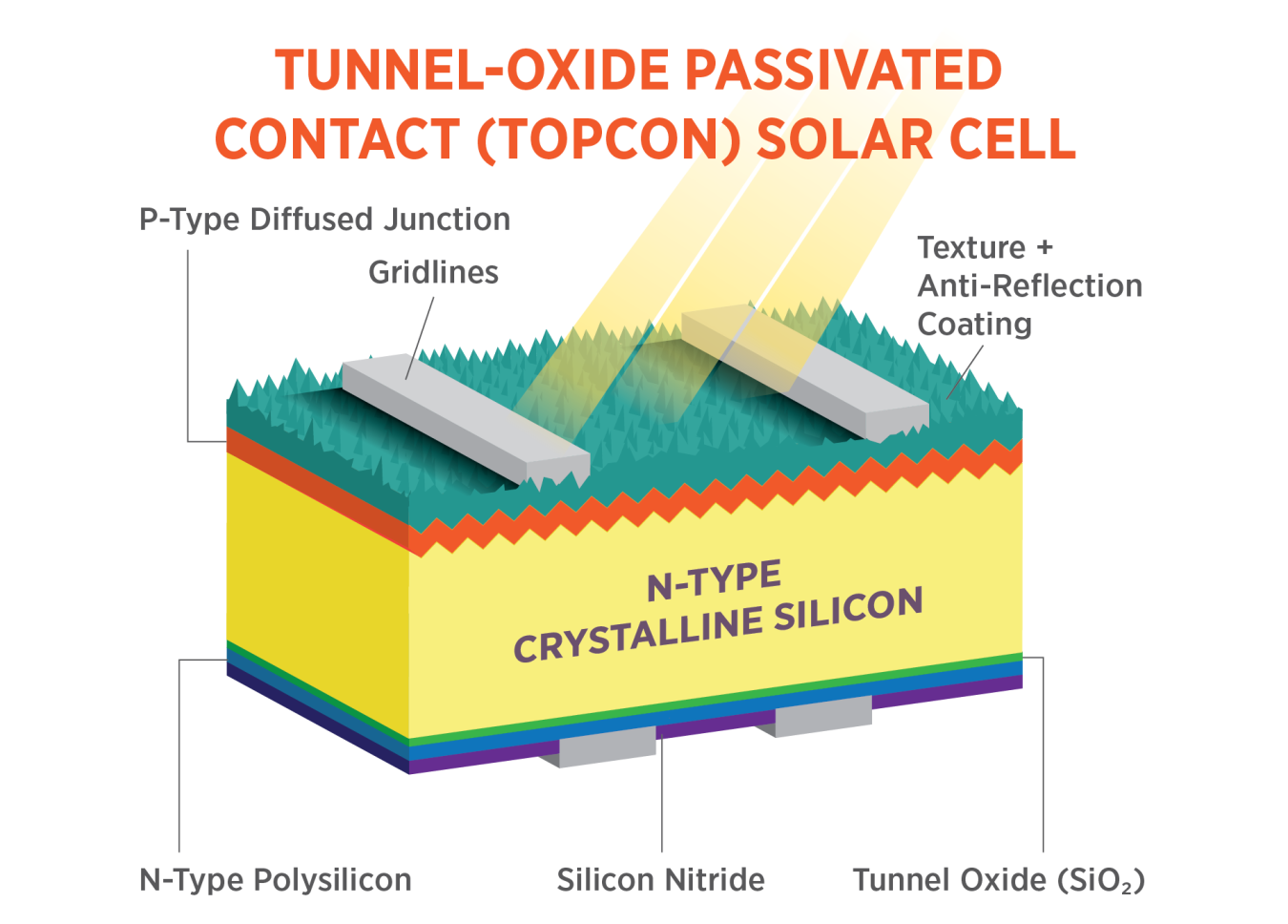
Another transition is taking place from PERC designs to “n-type” technologies such as silicon heterojunctions (SHJ) and tunnel-oxide passivated contacts (TOPCon). This transition to n-type cells is also driven by efficiency improvements.
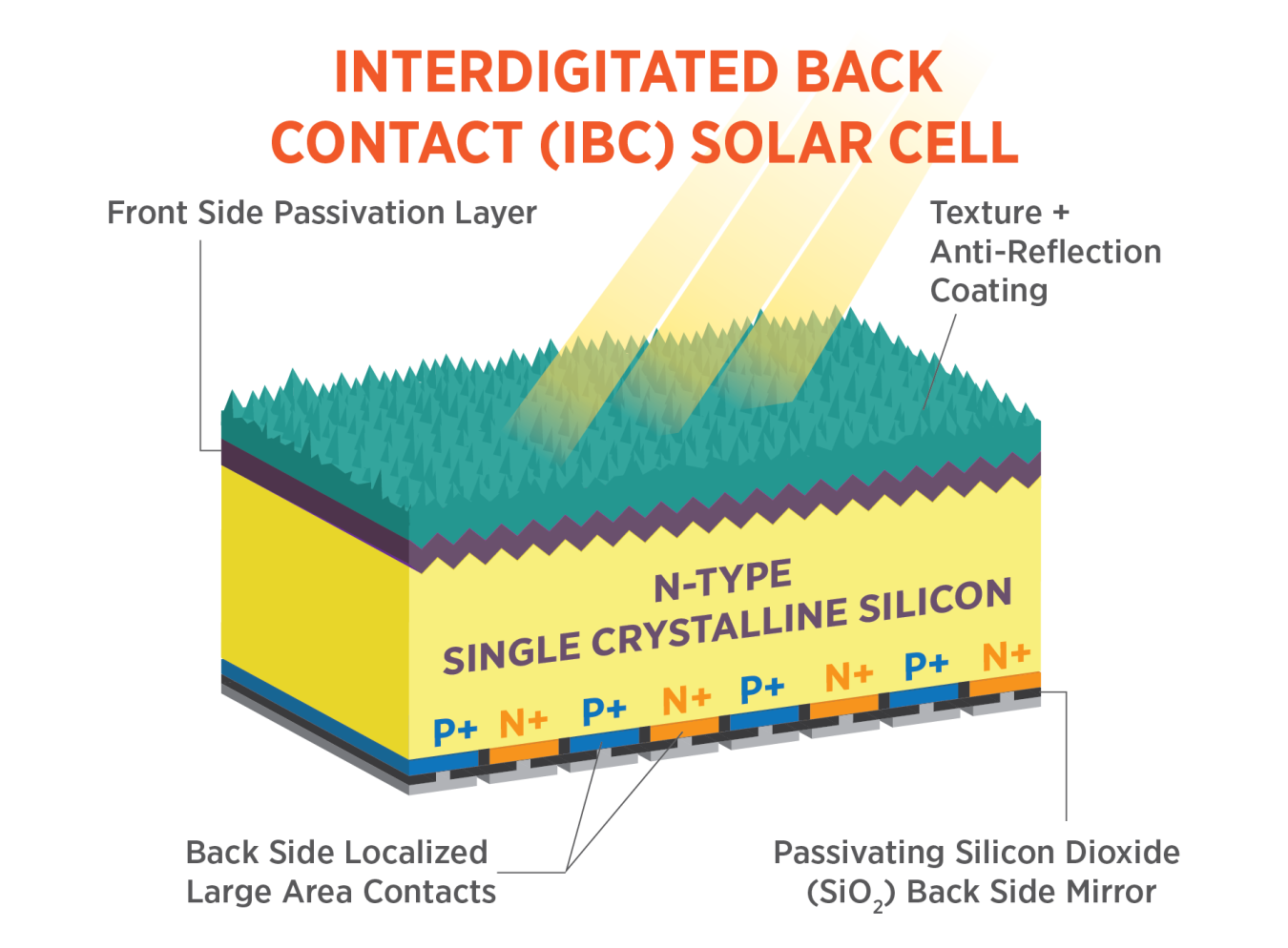
Additionally, interdigitated back contact (IBC) cells are an advanced technology where all the metal contacts to the silicon cell are placed on the back surface. This means there is no light blocked by the presence of metal on the front surface of the cell. IBC designs are more complicated to manufacture, so they currently represent only a small fraction of crystalline silicon solar cell production.
What are SETO Research Priorities in Crystalline Silicon?
Current SETO research efforts focus on innovative ways to reduce costs, increase the efficiency, and reduce environmental impact of silicon solar cells and modules. This includes the advancement of new technologies using n-type wafers, optimization of recycling processes, understanding degradation in silicon modules and integration of silicon cells into tandem architectures with other materials. Learn about active SETO funding programs that incorporate silicon PV research:
- Small Innovative Projects in Solar (SIPS): Concentrating Solar-Thermal Power and Photovoltaics
- Photovoltaics Research and Development (PVRD) Funding Program
- Materials, Operation, and Recycling of Photovoltaics (MORE PV) Funding Program
- Bipartisan Infrastructure Law Silicon Solar Manufacturing and Dual-use Photovoltaics Incubator
What are the Benefits of Crystalline Silicon Solar Cells?
| Maturity | Silicon solar cells are well understood, and their manufacturing process is highly optimized. |
| Performance | Industrially produced silicon cells offer higher efficiencies than any other mass-produced single-junction device. Higher efficiencies reduce the cost of the final installation because fewer solar cells need to be manufactured and installed for a given output. |
| Reliability | Crystalline silicon cells reach module life spans of 25+ years and exhibit power degradation less than 1% a year. |
| Abundance | Silicon is the second most abundant element in Earth's crust (after oxygen). |
Learn more about SETO’s PV research and how PV technologies work.