
Since its invention in the early 1990s, the Indium Gallium Nitride (InGaN) LED has revolutionized the world of lighting by providing unparalleled efficiency and a host of different applications from automotive and home lighting to lasers and displays. While blue LEDs have achieved spectacular efficiencies, longer wavelength InGaN LEDs like red and green have lagged behind. Emerging applications such as micro-LED RGB displays will require highly efficient long-wavelength light sources, and InGaN LEDs remain a leading candidate if some of the fundamental material challenges can be overcome.
Researchers at the University of California Santa Barbara are using advanced material growth, material characterization, and device fabrication to study some of these fundamental challenges and advance the scientific knowledge on red and green InGaN LEDs. Using metal organic chemical vapor deposition, this project is growing GaN-based long-wavelength LEDs on sapphire (one of the leading industrial substrates for LED growth) and using transmission electron microscopy (TEM) to study a special kind of naturally occurring crystallographic defect known as V-defects. V-defects are believed by many in the LED industry to be the key to engineering the next generation of long-wavelength GaN-based LEDs.
Achieving high efficiency in LEDs is all about maximizing the number of carriers (electrons and holes) that produce light (radiative recombination) and minimizing all parasitic recombination processes. These parasitic recombination processes include Shockley-Read-Hall (SRH) and Trap-Assisted Auger Recombination (TAAR), both of which are being studied extensively at UCSB with the support of the DOE. The figure below shows a TEM image with both ‘large’ and ‘small’ V-defects. Recent results published from UCSB showed that reducing the number of ‘small’ V-defects in long-wavelength InGaN LEDs increased efficiency, which is likely due to these small V-defects being SRH and TAAR centers. Large V-defects are generally considered beneficial if properly engineered, as they help carriers "inject" into the quantum wells where the LEDs produce light.
Ongoing research is looking at the material science and kinetics of V-defect formation, which will inform both academic and industry efforts to utilize V-defects in next-generation green InGaN LEDs. Results from this research effort can then be applied to improve longer-wavelength InGaN LEDs. Additionally, novel devices are being created and studied to understand TAAR, SRH, and other critical processes in green LEDs. (September 2022)
Return to Research Highlights.
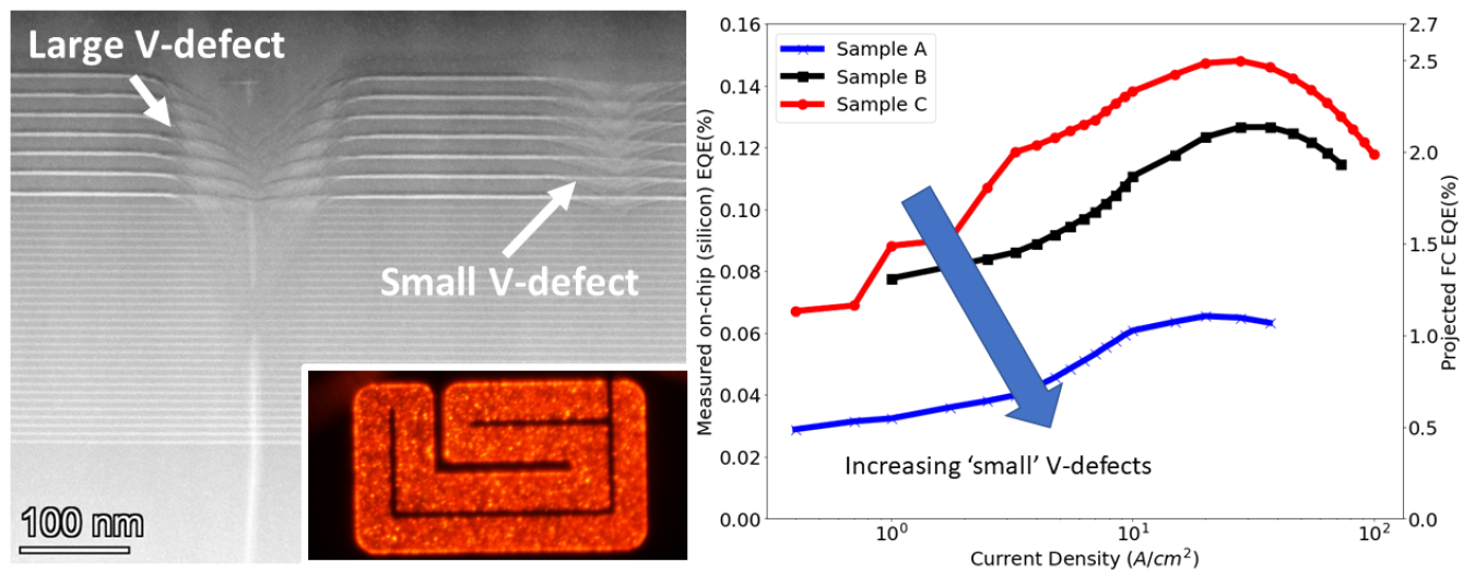
Left: cross-section transmission electron microscopy image showing large (desirable) and small (undesirable) V-defects. Left inset: light emission from a UCSB red LED. Right: graph showing decrease of efficiency with increasing density of small V-defects.