
Simulations are used to predict the performance and behavior of a system instead of relying solely on experimental understanding – thus reducing cost and shortening development time. With the help of DOE funding, researchers at the University of California at Santa Barbara (UCSB), in collaboration with those at National Taiwan University, the University of Minnesota, and France’s École Polytechnique, have developed a numerical tool that allows the 3D simulation of Group III nitride devices.
Because simulations of semiconductor devices such as LEDs are much more challenging than optical simulations, relatively few simulation tools are commercially available – and those that are available are restricted to 1D or 2D descriptions of the devices. Additionally, Group III nitride semiconductor materials present further challenges in accurate materials property descriptions, when compared to a conventional Group III-V semiconductor systems such as GaAs, because of the random alloy fluctuations of the nitride alloys (InGaN, AlGaN, and InAlN) present in all nitride LEDs.
The researchers are now testing and using the new simulation tool to guide their epitaxy design of efficient green nitride LEDs. Recently, they demonstrated the understated impact of the number of quantum wells on the devices' performance and are now working on advanced designs to evenly distribute carriers in all quantum wells of the structure, which will reduce current density droop in LEDs, thus providing better performance across the operating range.
A promising path of LED design could be to replace the conventional GaN quantum barriers of the active region that separate the quantum wells with InGaN alloy barriers. The researchers found that even small amounts of indium in the barriers opens percolative transport paths that locally lower the energy barrier for carriers propagation. The other existing 1D simulators could not capture this behavior, as they can’t describe the 3D nature of fluctuations – unlike these 3D simulations, which predict behaviors similar to those observed by the researchers. (May 2019)
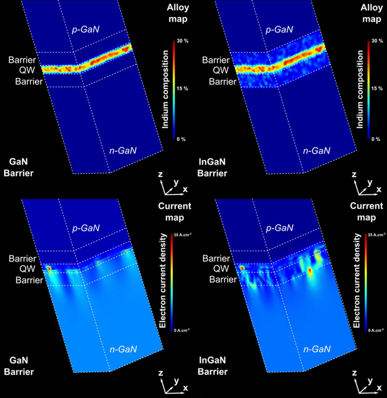
Simulated alloy map of green LED c-plane with (top left) GaN barriers and (top right) In0.04Ga0.96N barriers. Bottom: Electron current density map at 10 A.cm‑2 for (l) GaN and (r) In0.04Ga0.96N barriers.
Return to Research Highlights.