
DOE supports innovative research focused on overcoming the current technological and commercial barriers for copper indium gallium diselenide [Cu(InxGa1-x)Se2], or CIGS, solar cells. A list of current projects, summary of the benefits, and discussion on the production and manufacturing of this solar technology are below.
Background
Since its initial development, copper indium diselenide (CuInSe2) thin-film technology has been considered promising for solar cells because of its favorable electronic and optical properties. It was later found that by substituting gallium (Ga) for indium (In), the bandgap can be increased from about 1.04 electron-volts (eV) for copper indium diselenide (CIS) films to about 1.68 eV for copper gallium diselenide (CGS) films. Optimal devices have been fabricated with only a partial substitution of Ga for In, leading to a substantial increase in overall efficiency and more optimal bandgap. These solar cells are commonly known as a copper indium gallium diselenide [Cu(InxGa1-x)Se2], or CIGS, cells.
Although laboratory-scale cell efficiencies have exceeded 20%, commercial CIGS modules typically have efficiencies between 12% and 14%.
Research Directions
Learn more about the DOE Solar Energy Technologies Office awardees and the projects involving CIGS below.
- Case Western Reserve University (Photovoltaics Research and Development: Small Innovative Projects in Solar)
- Arizona State University (Bridging Research Interactions through collaborative Development Grants in Energy)
- Lawrence Livermore National Laboratory (Bridging Research Interactions through collaborative Development Grants in Energy)
- National Renewable Energy Laboratory (Foundational Program to Advance Cell Efficiency)
- National Renewable Energy Laboratory (Bridging Research Interactions through collaborative Development Grants in Energy)
- Old Dominion University (Foundational Program to Advance Cell Efficiency)
- Sandia National Laboratory (Bridging Research Interactions through collaborative Development Grants in Energy)
- Stanford University (Bridging Research Interactions through collaborative Development Grants in Energy)
- U.S. Photovoltaic Manufacturing Consortium (Photovoltaic Manufacturing Initiative Part I)
- University of Delaware (Foundational Program to Advance Cell Efficiency)
- University of Delaware (Next Generation Photovoltaics II Projects)
- University of Minnesota (Next Generation Photovoltaics II Projects)
Benefits
The benefits of CIGS solar cells include:
- High absorption: This direct-bandgap material can absorb a significant portion of the solar spectrum, enabling it to achieve the highest efficiency of any thin-film technology.
- Tandem design: A tunable bandgap allows the possibility of tandem CIGS devices.
- Protective buffer layer: The grain boundaries form an inherent buffer layer, preventing surface recombination and allowing for films with grain sizes of less than 1 micrometer to be used in device fabrication.
Production
Two of the low-cost deposition methods that produce the highest device and module efficiencies were developed in the 1980s. These methods are:
- Co-evaporation, in which precursor elements are allowed to sublimate in a high-vacuum environment and then re-deposit on a heated substrate.
- Precursor Reaction Processes, in which a precursor containing Cu and In/Ga is deposited at a low temperature by any of several processes, such as sputtering or electroplating. This is followed by a reactive annealing step in a Se compound, such as hydrogen selenide (H2Se) or gaseous selenium (Se), to form CIGS films. This is also commonly known as two-stage deposition; a variant of this technique, three-stage deposition, is also commonly used.
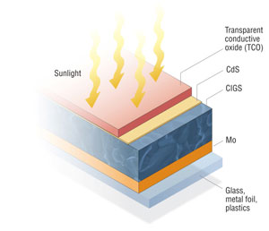
After the CIGS deposition, the junction is formed by chemical-bath deposition of the n-type CdS layer. To finish the solar cell, a high-resistance zinc oxide (ZnO) layer and a high-conductivity n+-type ZnO layer are deposited by either sputtering or chemical-vapor deposition. Laser-scribing processes at different steps in the production process create the individual solar cells connected in series.
Alternative manufacturing techniques have been explored, such as reactive sputtering, magnetron sputtering (Cu, In, and Ga are sputtered while Se is evaporated), and electrodeposition. However, co-evaporation and precursor reaction processes still remain the most popular.
A major increase in device performance was achieved when the ceramic or borosilicate glass substrate was replaced by soda-lime glass. Although soda-lime glass was chosen because it has closer thermal expansion properties to CIGS, it was ultimately determined that the primary advantage of using soda-lime glass results from the diffusion of sodium (Na) ions from the glass into the CIGS absorber layer. Work is currently being done to identify the role of Na in improving CIGS performance and what tolerances CIGS has to the inclusion of Na. Current manufacturing techniques incorporate Na either from soda-lime glass or a separate Na source. Soda-lime glass has an added advantage of being less expensive than previous glass substrates.
All high‐efficiency CIS and CIGS devices use molybdenum (Mo) as the back contact primarily because of its work function and the high reflectivity of the Mo film. These films are typically deposited through direct-current (DC) sputtering. The sputtering deposition process requires precise pressure to control the stress in the film. Because of some inherent problems with the Mo back-contact, such as the possibility of a hole-blocking Schottky diode effect at the interface, other metals have been investigated to replace Mo, but have had limited success.
For more information on CIGS solar cells, visit the Energy Basics website.